| �� |
|
|
|
��Ʒ���
|
•
Optical format : 1/3-inch (5:4)
• Active imager size : 4.6mm(H) x 3.7mm(V),5.9mm
diagonal
• Active pixels : 1280H x 1024V
• Pixel size : 3.6 x 3.6µm
• Color filter array : RGB Bayer pattern
• Shutter type : Electronic rolling shutter
(ERS)
• Maximum data rate/master clock : 27 MPS/54 MHz
• Frame rate :
QSXGA (2048 x 1536) 15 fps at 54 MHz
VGA (640 x 480) 30 fps at 54 MHz
• Maximum resolution at 60 fps/54 MHz clock :
640 x 512
• ADC resolution : 10-bit, dual on-chip
• Responsivity : 1.0 V/lux-sec (550nm)
• Dynamic range : 71dB
• SNRMAX : 44dB
• Supply Voltage :
I/O digital 1.8�C3.1V
Core digital 2.5�C3.1V
Analog 2.5�C3.1V
• Power consumption : 170mW SXGA at 15 fps (54
MHz EXTCLK)
• Operating temperature :�C30��C to +70��C
• Packaging : 44-ball iCSP; 48-pin CLCC |
|
��Ʒ����
|
•
DigitalClarity® CMOS imaging technology
• System-on-a-Chip (SOC)��Completely integrated
camera system
• Ultra-low power, high fidelity, progressive
scan CMOS image sensor
• Superior low-light performance
• On-chip image flow processor (IFP) performs
sophisticated processing:
�C Color recovery and correction
�C Sharpening, gamma, lens shading correction
�C On-the-fly defect correction
• Electronic pan, tilt, and zoom
• Automatic features:
�C Auto exposure, auto white balance (AWB), auto
black reference (ABR), auto flicker avoidance,
auto color saturation, auto defect
identification and correction
�C Fully automatic Xenon and LED-type flash
support
• Fast exposure adaptation
• Multiple parameter contexts
• Easy and fast mode switching
• Camera control sequencer automates:
�C Snapshots
�C Snapshots with flash
�C Video clips
• Simple two-wire serial programming interface
• ITU-R BT.656 (YCbCr), 565RGB, 555RGB, or
444RGB formats (progressive scan)
• Raw and processed Bayer formats
• Output FIFO and integer clock divider:
��Uniform pixel clocking |
|
��ƷӦ��
|
• Security
• Biometrics
• Video conferencing
• Toys |
|
���ֽ���
|
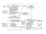
The MT9M131
features DigitalClarity™, Aptina��s breakthrough,
low-noise CMOS imaging technology that achieves
CCD image quality (based on signal-to-noise
ratio and low-light sensitivity) while
maintaining the inherent size, cost and
integration advantages of CMOS.The MT9M131
performs sophisticated processing functions
including color recovery,
color correction, sharpening, programmable gamma
correction, auto black reference clamping, auto
exposure, automatic 50Hz/60Hz flicker avoidance,
lens shading correction, auto white balance
(AWB), and on-the-fly defect identification and
correction.
Additional features include day/night mode
configurations; special camera effects such as
sepia tone and solarization; and interpolation
to arbitrary image size with continuous filtered
zoom and pan. The device supports both Xenon and
LED-type flash light sources in several snapshot
modes.
The MT9M131 can be programmed to output
progressive-scan images up to 30 frames per
second (fps) in preview power-saving mode, and
15 fps in full-resolution (SXGA) mode. In either
mode, the image data can be output in any one of
six 8-bit formats:
• ITU-R BT.656 (formerly CCIR656, progressive
scan only) YCbCr
• 565RGB
• 555RGB
• 444RGB
• Raw Bayer
• Processed Bayer
The FRAME_VALID (FV) and LINE_VALID (LV) signals
are output on dedicated signals, along with a
pixel clock that is synchronous with valid data. |
|
�� |
|
��
|
|
|
��Ʒ���
|
•
Optical format : 1/3-inch
• Active imager size : 4.51mm(H) x 2.88mm(V)
5.35mm diagonal
• Active pixels : 752H x 480V
• Pixel size : 6.0µm x 6.0µm
• Color filter array : Monochrome or color RGB
Bayer pattern
• Shutter type Global shutter��TrueSNAP™
• Maximum data rate/master clock : 26.6 MPS/26.6
MHz
• Full resolution : 752 x 480
• Frame rate : 60 fps (at full resolution)
• ADC resolution : 10-bit column-parallel
• Responsivity : 4.8 V/lux-sec (550nm)
• Dynamic range :
>55dB linear;
>80dB−100dB in HiDy mode
• Supply voltage : 3.3V +0.3V (all supplies)
• Power consumption :
<320mW at maximum data rate
100µW standby power
• Operating temperature :�C30��C to +70��C
• Packaging : 48-pin CLCC |
|
��Ʒ����
|
• Aptina®
DigitalClarity® CMOS imaging technology
• Array format: Wide-VGA, active 752H x 480V
(360,960 pixels)
• Global shutter photodiode pixels; simultaneous
integration and readout
• Monochrome or color: Near_IR enhanced
performance for use with non-visible NIR
illumination
• Readout modes: Progressive or interlaced
• Shutter efficiency: >99%
• Simple two-wire serial interface
• Register lock capability
• Window size: User programmable to any smaller
format (QVGA, CIF, QCIF, and so on). Data rate
can be maintained independent of window size
• Binning: 2 x 2 and 4 x 4 of the full
resolution
• ADC: On-chip, 10-bit column-parallel (option
to operate in 12-bit to 10-bit companding mode)
• Automatic controls: Auto exposure control
(AEC) and auto gain control (AGC); variable
regional and variable weight AEC/AGC
• Support for four unique serial control
register IDs to control multiple imagers on the
same bus
• Data output formats:
• Single sensor mode:
�� 10-bit parallel/stand-alone
�� 8-bit or 10-bit serial LVDS
• Stereo sensor mode:
�� Interspersed 8-bit serial LVDS |
|
��ƷӦ��
|
• Security
• High dynamic range imaging
• Unattended surveillance
• Stereo vision
• Video as input
• Machine vision
• Automation |
|
���ֽ���
|
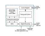
The Aptina
Imaging MT9V032 is a 1/3-inch wide-VGA format
CMOS active-pixel digital image sensor with
global shutter and high dynamic range (HDR)
operation. The sensor has specifically been
designed to support the demanding interior and
exterior unattended surveillance imaging needs,
which makes this part ideal for a wide variety
of imaging applications in real-world
environments.
This wide-VGA CMOS image sensor features Digital
Clarity Aptina��s breakthrough low-noise CMOS
imaging technology that achieves CCD image
quality (based on signal to-noise ratio and
low-light sensitivity) while maintaining the
inherent size, cost, and integration advantages
of CMOS.
The active imaging pixel array is 752H x 480V.
It incorporates sophisticated camera functions
on-chip��such as binning 2 x 2 and 4 x 4, to
improve sensitivity when operating in smaller
resolutions��as well as windowing, column and row
mirroring. It is programmable through a simple
two-wire serial interface.
The MT9V032 can be operated in its default mode
or be programmed for frame size, exposure, gain
setting, and other parameters. The default mode
outputs a wide-VGA size image at 60 frames per
second (fps). |
|
�� |
|
��
|
|
|
��Ʒ���
|
•
Optical Format:1/4-inch (4:3)
• Active Imager Size: 3.58mm(H) x 2.69mm(V)
4.48mm (Diagonal)
• Active Pixels: 640H x 480V (VGA)
• Pixel Size: 5.6µm x 5.6µm
• Color Filter Array: RGB Bayer Pattern
• Shutter Type: Electronic Rolling Shutter (ERS)
• Maximum Data Rate/Master Clock:
�� 12−13.5 Mp/s/
�� 24−27 MHz
• Frame Rate:
�� VGA (640 x 480) 15 fps at 12 MHz (default),
programmable up to 30 fps at 27 MHz
�� CIF (352 x 288) Programmable up to 60 fps
�� QVGA (320 x 240) Programmable up to 90 fps
• ADC Resolution: 10-bit, on-chip
• Responsivity: 1.9 V/lux-sec (550nm)
• Dynamic Range: 60dB
• SNRMAX: 45dB
• Supply Voltage: 2.8V +0.25V
• Power Consumption <80mW at 2.8V, 15 fps at
12MHz
• Operating Temperature: -20��C to +60��C
• Packaging: 44-Pin ICSP, 48-Pin CLC |
|
��Ʒ����
|
• Aptina®
DigitalClarity® CMOS imaging technology
• System-On-a-Chip (SOC)��Completely integrated
camera system
• Ultra low-power, high fidelity CMOS image
sensor
• Superior low-light performance
• Up to 30 fps progressive scan at 27 MHz for
high quality video at VGA resolution
• On-chip image flow processor (IFP) performs
sophisticated processing: color recovery and
correction, sharpening, gamma, lens shading
correction, on-the-fly defect correction, 2X
fixed zoom
• Automatic exposure, white balance and black
compensation, flicker avoidance, color
saturation, and defect identification and
correction, auto frame rate, back light
compensation
• Xenon and LED-type flash support
• Two-wire serial programming interface
• Progressive scan ITU_R BT.656 (YCbCr), YUV,
565RGB, 555RGB, and 444RGB output data formats |
|
��ƷӦ��
|
• Security
• Biometrics
• Network cameras
• Toys and other battery-powered products |
|
���ֽ���
|
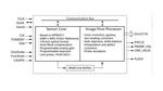
This SOC VGA
CMOS image sensor features DigitalClarity
Aptina��s breakthrough, low-noise CMOS imaging
technology that achieves CCD image quality
(based on signal to-noise ratio and low-light
sensitivity) while maintaining the inherent
size, cost, and integration advantages of CMOS.
The MT9V131 is a fully-automatic, single-chip
camera, requiring only a power supply, lens, and
clock source for basic operation. Output video
is streamed through a parallel 8-bit port, as
shown in Figure 2 on page 3. Output pixel clock
is used to latch the data, while FRAME_VALID and
LINE_VALID signals indicate the active video.
The sensor can be put in an ultra-low power
sleep mode by asserting the STANDBY pin. Output
pads can also be tri-stated by de-asserting the
OE# pin. The MT9V131 internal registers can be
configured using a two-wire serial interface.
The MT9V131 can be programmed to output
progressive scan images up to 30 fps in an 8-bit
ITU_R BT.656 (YCbCr) formerly CCIR656, YUV,
565RGB, 555RGB, or 444RGB formats. The
FRAME_VALID and LINE_VALID signals are output on
dedicated pins, along with a pixel clock that is
synchronous with valid data. |
|
�� |
|
��
|
|
|
��Ʒ���
|
•
Optical format: 1/4-inch (4:3)
• Active imager size: 3.63mm(H) x
2.78mm(V)4.57mm diagonal
• Active pixels: 640H x 480V
• NTSC output: 720H x 486V
• PAL output: 720H x 576V
• Pixel size: 5.6µm x 5.6µm
• Color filter array: RGB paired Bayer pattern
• Shutter type: Electronic rolling shutter (ERS)
• Maximum data rate/master clock:
�� 13.5 Mp/s
�� 27 MHz
• Frame rate (VGA 640H x 480V) :30 fps at 27 MHz
(NTSC) 25 fps at 27 MHz (PAL)
• Integration time:
�� 16µs�C33ms (NTSC)
�� 16µs�C40ms (PAL)
• ADC resolution: 10-bit, on-chip
• Responsivity: 5 V/lux-sec (550nm)
• Pixel dynamic range : 70dB
• SNRMAX :39dB
• Supply voltage :
�� I/O digital 2.5�C3.1V(2.8V nominal)
�� Core digital 2.5�C3.1V(2.8V nominal)
�� Analog 2.5�C3.1V(2.8V nominal)
• Power consumption1:
�� Operating 320mW
�� Standby 0.56mW
• Operating temperature 1: �C30��C to +70��C
• Package: 48-pin CLCC |
|
��Ʒ����
|
•
DigitalClarity® CMOS imaging technology
• System-on-a-chip (SOC)��completely integrated
camera system
• NTSC and PAL (true two field) analog composite
video output
• Low power, interlaced scan CMOS image sensor
• ITU-R BT.656 parallel output (8-bit,
interlaced)
• Serial LVDS data output
• Supports use of external devices for addition
of custom overlay graphics
• Superior low-light performance
• On-chip image flow processor (IFP) performs
sophisticated processing
• Color recovery and correction, sharpening,
gamma, lens shading correction, and on-the-fly
defect correction
• Automatic Features: Auto exposure (AE), auto
white balance (AWB), auto black reference (ABR),
auto flicker avoidance, auto color saturation,
and auto defect identification and correction
• Simple two-wire serial programming interface |
|
��ƷӦ��
|
• 900 MHz and
2.4 GHz wireless cameras
• Composite video and digital video out cameras
• CCTV security cameras
• Consumer video products
• Smart cameras
• Evidence quality cameras
• Cameras with the need for active or passive
overlay |
|
���ֽ���
|
The Aptina
Imaging MT9V135 is a VGA-format, single-chip
camera CMOS active-pixel digital image sensor.
It captures high-quality color images at VGA
resolution and outputs NTSC or PAL interlaced
composite video and CCIR 656 digital composite
video.
This VGA CMOS image sensor features Aptina��s
breakthrough DigitalClarity® technology a
low-noise CMOS imaging technology that achieves
CCD image quality (based on signal-to-noise
ratio and low-light sensitivity) while
maintaining the inherent size, cost, low-power,
and integration advantages of CMOS.
The sensor is a complete camera-on-a-chip
solution. It incorporates sophisticated camera
functions on-chip and is programmable through a
simple two-wire serial interface.
The MT9V135 performs sophisticated processing
functions including color recovery, color
correction, sharpening, programmable gamma
correction, auto black reference clamping, auto
exposure, automatic 50/60Hz flicker avoidance,
lens shading correction, auto white balance
(AWB), and on-the-fly defect identification and
correction.
The MT9V135 outputs interlaced-scan images at 30
or 25 fps, supporting both NTSC and PAL video
formats. |
|
�� |
|
��
|
|
|
��Ʒ���
|
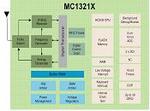
•ZigBee is a networking protocol operating at
868/915 MHz & 2.4 GHz spectrum with IEEE®
802.15.4 MAC
•ZigBee enables simplicity, long battery life,
networking capabilities, reliability, and low
system cost |
|
��Ʒ����
|
• Supports
MC1319x, MC1320x,
MC1321x
• Supports HCS08 8-bit MCU
• ZigBeeTM Compliant Platform
• Supports Star, Tree, & Mesh NWKs
• Established Routing Algorithm
• Network Formation, Recovery, and
Healing
• Device Interoperability
• Clusters: Standard Interfaces for
Actuators & Sensors
• Stack Provided in Header Files &
Libraries
• Sample Applications and Platform
Code Provided in Source |
|
��ƷӦ��
|
•ZigBee is
excellent for remote monitoring and control and
sensory network applications
• ZigBee targets residential and commercial
control and monitoring, utilities, medical and
handheld markets. |
|
���ֽ���
|
ZigBee relies
upon the robust IEEE 802.15.4 PHY/MAC to provide
reliable data transfer in noisy,
interference-rich environments
•Message acknowledgement and an optional beacon
structure
•Multi-level security
Ideal For
•Low data rate monitoring and control
applications that require a robust network
•Low latency, infrequent, low data rate and
small packet data
•Large area coverage
•Using the mesh networks that support 1000 of
devices
•Ultra low power monitoring applications that
operate for years on inexpensive alkaline
batteries
Not Ideal For
•Applications requiring long range without using
routers
•Mobile applications
•Being addressed in future revision
•Streaming data |
| �� |
|
��
|
|
|
��Ʒ���
|
��Sensitivity��42 dBV/Pa
��Signal to Noise��59 dB(A)
��Maximum Sound Pressure Level��110 Dbspl
��Supply Voltage��1.5 �C 3.3 V
��Current Consumption��70 ��A
��Lead free and halogen free package:Size��4.72 x
3.76 x 1.25 mm |
|
��Ʒ����
|
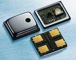
The Silicon
Microphone consists of two chips combined in a
single package.The MEMS chip is a capacitor made
up of a stiff and perforated backplate and a
flexible membrane on a Silicon substrate. It
transfers the sound waves into capacity
variations. The ASIC chip converts the capacity
variations into an electrical signal. |
|
��ƷӦ��
|
Infineon
SMM310 is optimized for consumer applications
with special focus on mobile
phones. Further application fields are notebooks
and cameras. The microphones are
also suitable for automotive, industrial or
medical applications, where microphones
are directly assembled onto the PCB and where
size as well as temperature immunity
matter. |
|
���ֽ���
|
Infineon
introduces the new product line Silicon
Microphone.The microphone sensors are based on
the new semiconductor MEMS(Micro Electro
Mechanical Systems) technology in contrast to
conventional microphones, which typically rely
on the electret condenser technology. |
|
�� |
|
��
|
|
|
��Ʒ���
|
TDA 525x - ASK/FSK ˫���շ��� Transceiver Family,
Frenquency 315,434, 868, 915MHz; sensitivity
-109dB. |
|
��Ʒ����
|
Ӣ�������߿����շ���ϵ����һ����ĵ�оƬ FSK/ASK �շ����������� 868
MHz��315 MHz��434 MHz �� 915 MHz Ƶ�εİ�˫������������ͨ�š� |
|
��ƷӦ��
|
���Ӱ�ȫ���,
���þ���ϵͳ, �������ߴ���ϵͳ, ����������ϵͳ |
|
���ֽ���
|
�ü��ɵ�·���м��ߵļ��ɶȣ�����ֻ��Ҫ�����ⲿ��������а�����Ч���ʷŴ��������� AGC
�ĵ���Ѷ�Ŵ�����LNA����˫ƽ���Ƶ�������ֱ��ת���������� RSSI ���ɵ� I/Q
��������FSK ���������ȫ���� VCO �Լ� PLL
�ϳ������ɵ��������������������˲��������ϱȽ�������Ƭ������������ֵ��������������ʼ���·��
2/3 ���»����Ž��� �����⣬�����жϵ繦�ܣ��Ӷ���ʡ������ġ� |
|
�� |
|
��
|
|
|
��Ʒ���
|
SmartLEWIS™ RX, TDA523x- Autonomous Multichannel
Receiver; Frequency 302-320, 434-450,
865-870MHz. ASK sensitivity -107dB@434MHz. |
|
��Ʒ����
|
Low Power, Low
Cost, Autonomous; suitable for all major short
range applications in the 315, 434, 868MHz
frequency bands |
|
��ƷӦ��
|
Remote Control
Systems, Security & Alarm Systems, Automated
Meter Reading (AMR), Home Automatic Systems, Low
Bit Rate Communication Systems, Remote Keyless
Entry (RKE), Tire Pressure Monitoring Systems
(TPMS) |
|
���ֽ���
|
Saving energy
wherever possible is our common goal. So, how to
do it if the system has to scan for information?
Well, just rest and consider TDA523x to be your
alarm clock. The SmartLEWIS TDA523x receiver
will scan for any news meant for the system and
just wake it up when something relevant is
available. If not, just continue to sleep��
��Low Power
Ultra Low System Power Consumption, especially
in park mode. While TDA523x is autonomously
polling for RF messages, the host
microcontroller can wait in lowest power sleep
mode for the End of Message interrupt, slowly
wake up and pick up the data from the data FIFO.
Reduced Processing Load; The host µC is
completely released from any processing of the
incoming bit-stream. ��Low Cost
Reduced System Costs, because a simpler and
cheaper host µC can be used, or the µC is able
to take over task which might require an
additional µC. Extremely Low SW Development
Effort
��Autonomous
TDA523x is an autonomous RF Receiver with an
integrated digital baseband. TDA523x takes over
the polling, and does the required filtering,
slicing, framing of the received data stream,
and makes the payload available via the data
FIFO. TDA523x is able to handle data from RKE
AND TPMS transmitters, even when they have
different modulation, bit rate, and data format.
TDA523x is widely configurable and allows easy
adaption to different tasks and requirements. |
|
�� |
|
��
|
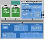
��TI -
TMS320DM6446 Processor�� |
|
|
|
��Ʒ���
|
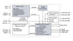
Core
ARM926EJ-S™ (MPU) Core
TMS320C64x+™ DSP Core
Memory
On-Chip L1/SRAM: 112 KB DSP, 40 KB ARM
On-Chip L2/SRAM: 64 KB DSP |
|
��Ʒ����
|
Video
Encode/Decode
H.264 BP D1 encoding, simultaneous H.264 BP CIF
coding
H.264 MP@L3, 30-fps SD decoding, VC1/WMV9 full
D1 SD decoding, MPEG-2 MP@ML SD decoding, MPEG-4
ASP full D1 SD decoding
Video Processing Subsystem
Front end �C Resizer, image processing engine,
16-bit digital input
Back end �C Integrated OSD, four video DACs,
24-bit digital RGB output
The Right Peripherals for Your Video, Audio,
Storage and Connectivity Needs
Package: 23mm X 23mm - 361-Pin BGA |
|
��ƷӦ��
|
Video
conferencing, video phones, video surveillance,
digital media adaptors and IP set-top boxes |
|
���ֽ���
|
The highly
integrated DM6446 Digital Video processor
enables OEMs and ODMs to quickly bring new
products to market at low consumer price points |
| �� |
|
��
|
|
|
��Ʒ���
|
4
channel, low power NTSC/PAL/SECAM video decoder.
Supports CVBS and S-video inputs.
Output in 8-bit ITU-R BT.656 format with
embedded syncs, or 8-bit 4:2:2 with discrete
syncs. Dual clocking interleaved 54 MHz data
output available. |
|
��Ʒ����
|
Low Power
(less than 720mW)
PNP package
Temp Range 0 ... 70C
Internal Phase-Locked Loop (PLL) for
Line-Locked Clock (Separate for Each Channel)
sampling |
|
��ƷӦ��
|
Surveillance
DVRs & Servers
Security Camera Systems
Large Format Video Wall Displays
Games Systems |
|
���ֽ���
|
The TVP5154 is
being positioned as a 4 Channel, Low Power Video
Decoder with Independent Scalers specifically
targeted at surveillance applications. |
|
|
